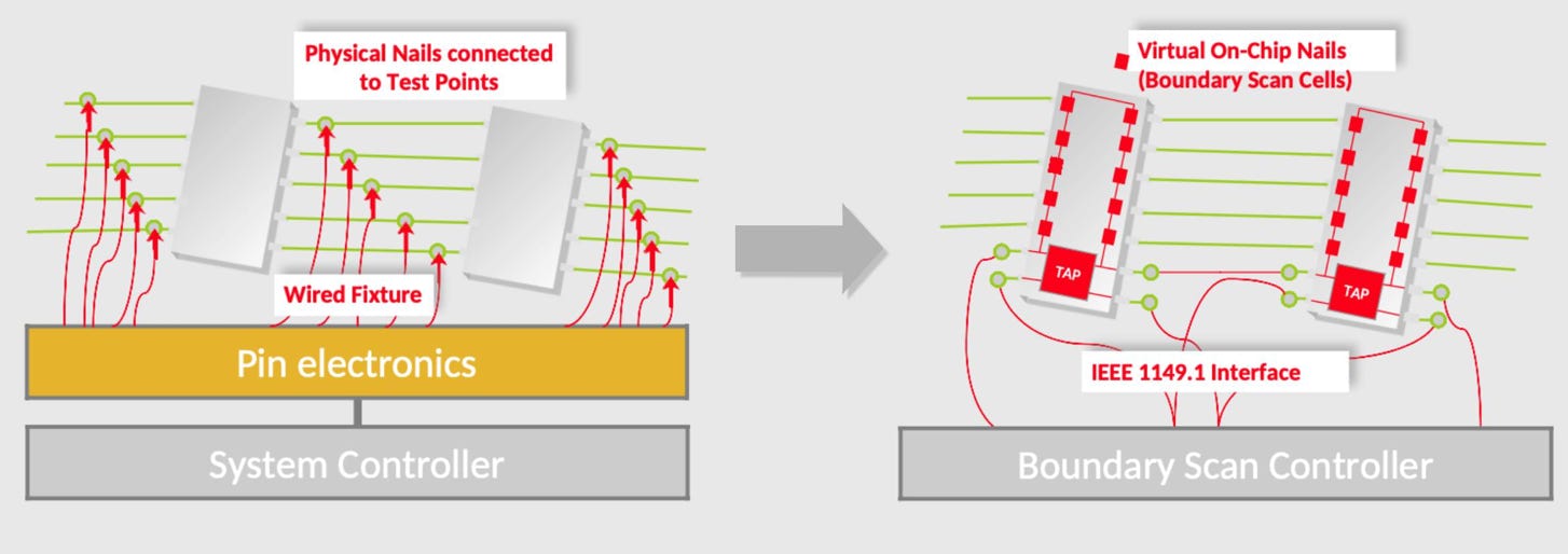
The idea of JTAG / Boundary Scan is to replace the test points (connected to physical nails of the ICT or Flying Probe tester) with virtual on-chip nails (integrated Boundary Scan cells in a Boundary Scan device).
Most processors, FPGAs, PLDs and many other complex devices support the boundary scan standard.
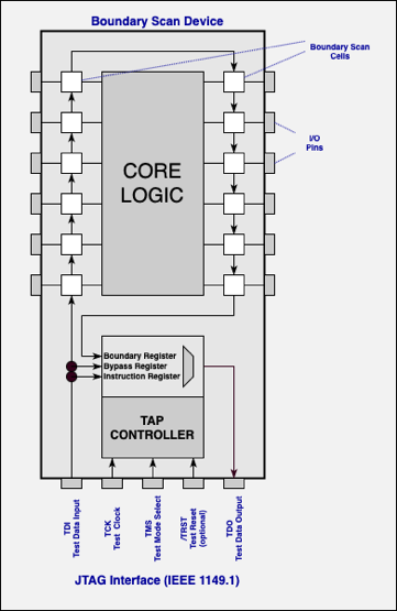
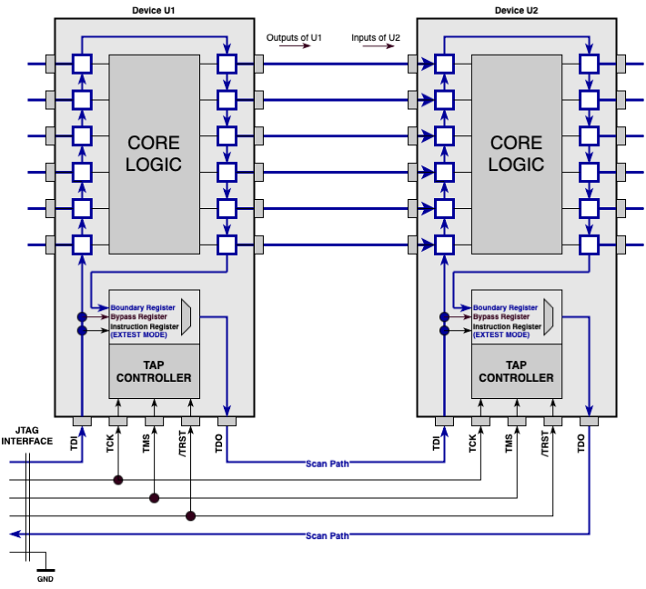
In addition to the core logic, a Boundary Scan Device contains the following components:
- The JTAG interface to control the Boundary Scan Device, consisting of a Test Data Input (TDI) and a Test Data Output (TDO), a Test Clock Input (TCK) and a Test Mode Select pin (TMS). A Test Reset input (/TRST) is optionally available.
- Boundary Scan Cells between the I/O Pins and the Core Logic. These Boundary Scan cells form the Boundary Register.
- A Bypass Register (1 bit).
- Optional additional Data Registers like an IDCODE Register (32 bit) or - for programmable Devices - a USERCODE Register (32 bit).
- An Instruction Register to select different operating modes of the device.
- A Test Access Port (TAP) Controller based on a state machine with 16 internal states, controlled by TMS and clocked by TCK.
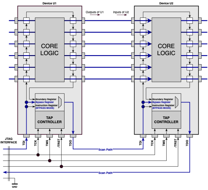
If there are several boundary scan devices on the board, they are typically connected in a scan chain. The TDO of one device is connected to the TDI of the next device. The signals TCK, TMS and /TRST (if available) will be connected in parallel. To simplify the access to the JTAG interface in most cases a test bus connector is used.
The following figure shows a simple example where some outputs of device U1 are connected to inputs of device U2. After switching on the power supply for the board, both components work in functional mode (BYPASS MODE), the boundary scan cells are bridged, the TDO outputs are connected to the TDI inputs via the 1 bit bypass register.
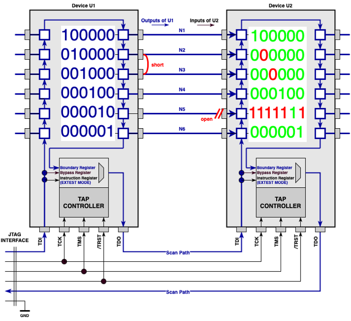
The board test via boundary scan takes place in the so-called EXTEST MODE. In this mode, the core logic is isolated and the I / O pins are connected directly to the boundary scan cells.
This is an example for testing the connections (N1… N6) between the boundary scan devices U1 and U2. Different patterns are output (U1) and measured at the inputs (U2). In this way, various faults (opens and shorts) can be found. The diagnosis is carried out at the pin and net level so that the actual error can be easily identified.